Update 2014-11-19: Thanks to the hackaday team for featuring my article on hackaday =-)
This blogpost shows you my recent overclocking experiments with the venerable Thinkpad 701 - a laptop from 1995 which has even made it to the MoMA collection. Why? Well, when it came out, the 701 was not only one of the first subnotebooks around, it was also the first subnotebook to feature a full-sized standard keyboard at the same time (and it still remains to be the only one btw). The engineers at IBM achieved this with an ingenious slide-mechanism which folded the keyboard together when the laptop lid was closed and they called their invention the "TrackWrite" keyboard. For its similarity with the folding of butterfly wings, the 701 became known as the Thinkpad butterfly.
Thinkpad 701 CPU specs
With the system´s original bus clock frequency set to 25 MHz, the 701 was either available with an Intel 486-DX2 which doubled this base frequency to 50 MHz, or with an Intel 486-DX4 which - against what the four in DX4 might suggest - only trippled it to 75 MHz. However, there was yet another inofficial configuration back then - the butterfly powered by a 133 MHz AM-5x86 CPU. It was a third-party modification which was offered by some specialized shops, e.g. by "Hantz & Partner" (at least according to the info from this thread). As for benchmarks, I recommend to read through the extensive X5 CPU comparisons conducted by David A. Ross on his webpage.
Mainboard details
The butterfly had two mainboards which acted as a single unit when connected together. As I have not found too much info about them I present some hardware details in the following paragraphs.
1. The bottom system board (BSB):
As seen from above:

A) TSB connector
B) OPTi 82C465 MVA, chipset controller chip (the mainboard design derives from this chip)
C) CHIPS F65545 B1, VGA controller chip
D) LC-display connectors
E) CIRRUS LOGIC CL-PD6720-QC-C, PCMCIA controller chip
F) PCMCIA connector
As seen from below:
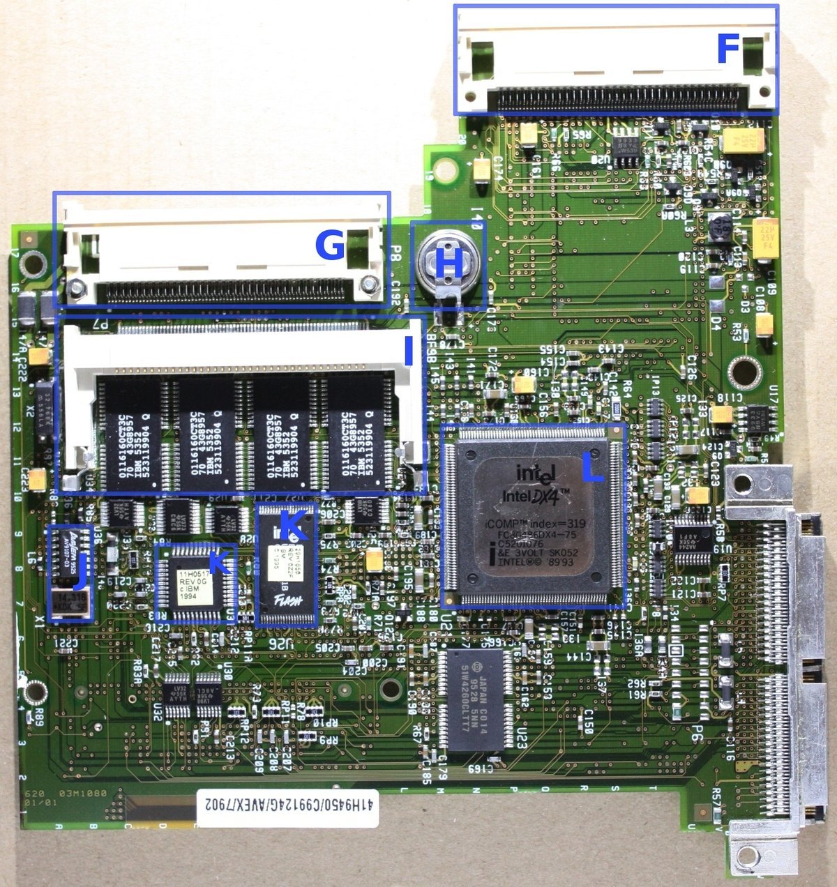
F) PCMCIA connector
G) HDD connector
H) BIOS battery (replace it with a new one, e.g. CR2025, if you want to save your board from corroding away in the future by leaking battery acid!)
I) 8 MB onboard RAM and RAM expansion slot (the latter is for up to 64 MB, thus maximum RAM will be 64+8 -> 72 MB)
J) AVASEM AV9107-03, CPU frequency generator chip (the 14.381 MHz oscillator crystal next to it provides the reference frequency btw)
K) Flash chips, probably for BIOS: Left ALTERA EPM7032V EEPROM labelled 11H0517, right Intel E28F004BL-T150 4-MBit Low-power boot block flash memory labelled 29H1850
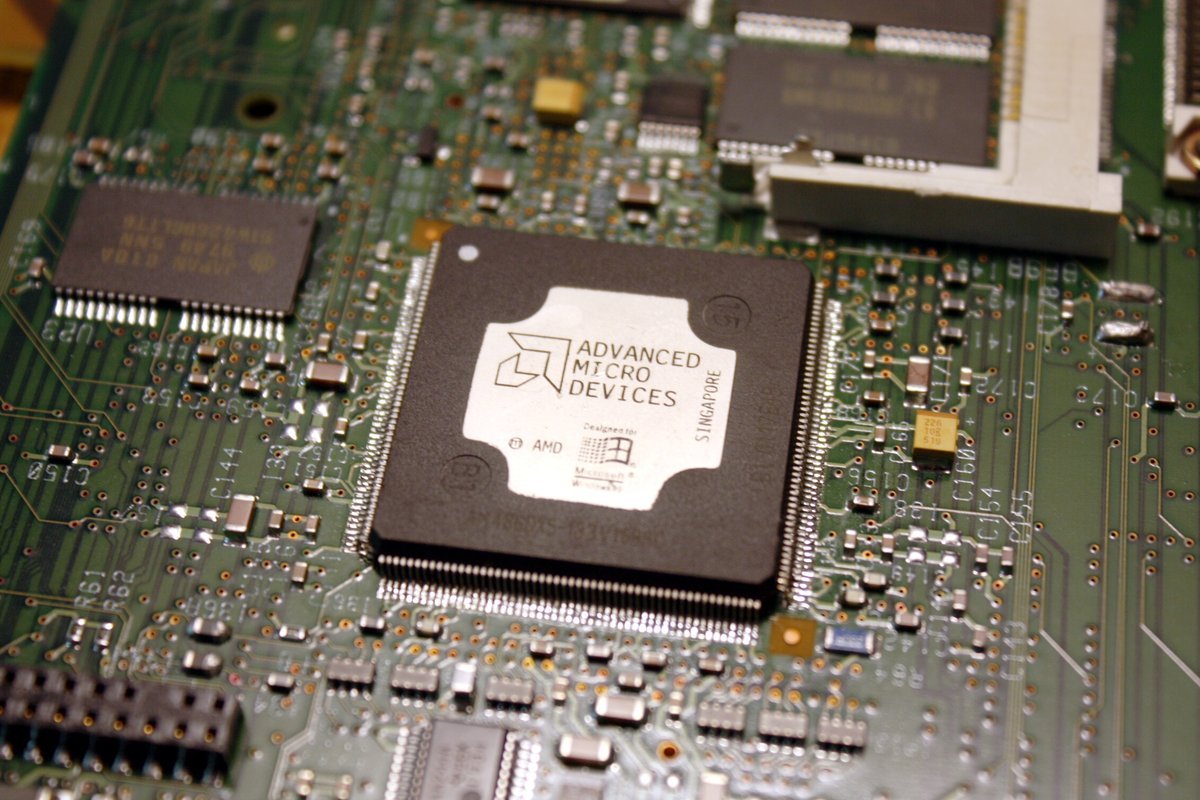
L) Intel 80486DX4-75 SK052, the CPU
2. The top system board (TSP):
As seen from below:
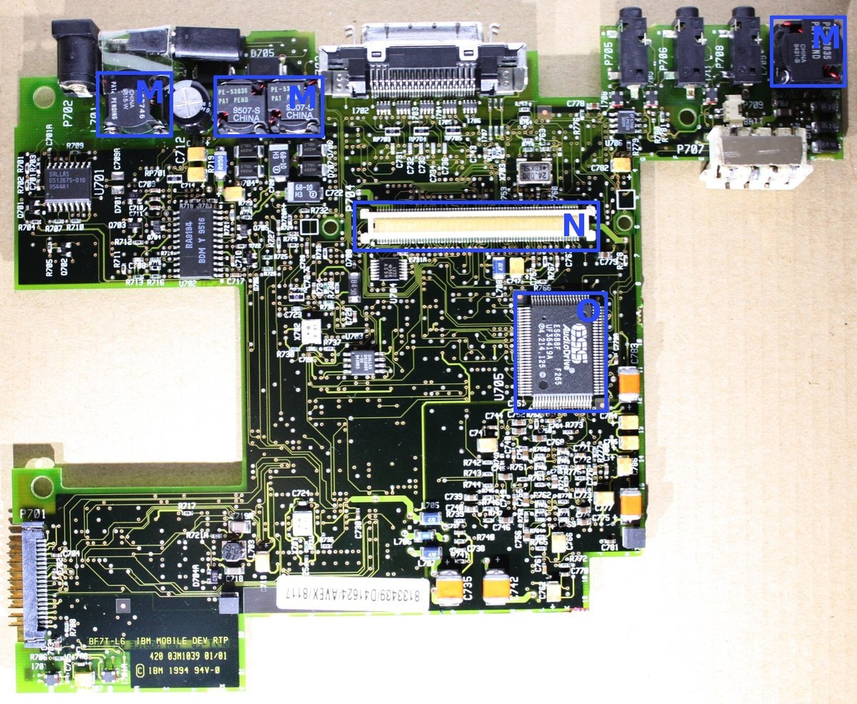
M) Coils (cold solder joints under these transformer coils - a realistic problem after almost 20 years - can cause the laptop not to power up, check them if your 701 doesn´t show any lifesign at all!)
N) BSB connector
O) ESS AudioDrive ES688F, audio controller chip
As seen from above:
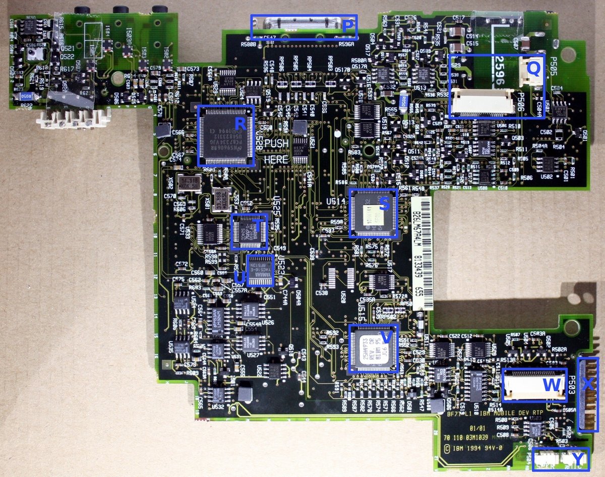
P) Floppy drive connector
Q) Keyboard connectors (the smaller one is for the Trackpoint a.k.a. the red dot)
R) PC87334VJG, controller chip for IEEE1284, parallel port and IDE interface (the 24.000 MHz reference crystal lies on the other side of the board)
S) Hitachi H8/3332 microcontroller labelled 10H4142
T) YAMAHA YMF289B, OPL3 FM synthesizer chip with 33.868 MHz reference crystal
U) YAMAHA YAC516-E, DAC16-L delta sigma modulation Digital-to-analog converter
V) Hitachi H8/3332 microcontroller labelled 25H4933
W) Keyboard connector
X) LCD inverter connector
Y) Internal speaker and microphone connectors
Some research work
To reverse-engineer how to get to a working Am5x86-powered Thinkpad 701 mainboard, I started to collect every info I could find about the X5 boards and 486 CPU overclocking in general. Some things I found out:
-
The X5 upgrade boards on the net (e.g. on ebay) include only the BSB -> thus the TSB must be irrelevant for successfully overclocking the butterfly. -> Consequently I purchased several additional BSBs for my Thinkpad 701C to tinker with them...
-
The 701´s BSB holds a Small Quad Flat Pack-208-pin CPU -> Only a fracture of the AMD 5x86 CPU family has this 208-pin package. There were several 168-pin upgrade kits for 80486 boards back in the 1990s which presumably had these chips soldered on top, e.g. known as "Turbochip" or "Evergreen" module. The chips were mostly labelled AMD Am5x86-P75 X5-133SFZ or AMD Am5x86-P75 DX5-133V16BHC -> I acquired both versios cheap on ebay...
-
In the (D)X5 the system clock is multiplied - no, not with five - but with four: 25.1 MHz * 4 -> 100.4 MHz in case of the butterfly. To get the full 133.3 MHz out of it requires to raise the bus clock speed from 25.1 to 33.3 MHz: 33.3 MHz * 4 -> 133.3 MHz.
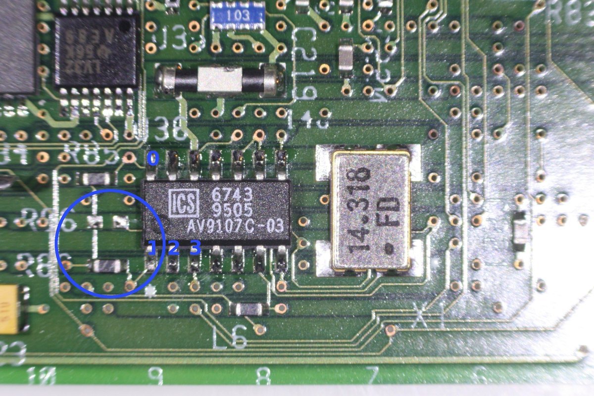
Overclocking the system bus
To raise the bus clock speed to the desired 33.3 MHz I searched for an oscillator circuit on the BSB - and I found one, a 14-pin AVASEM AV9107-03 clockspeed generator chip and a 14.318 MHz crystal next to it. According to its datasheet (thanks alldatasheet.com!) the chip uses the latter as a reference crystal to generate preprogrammed frequencies. Four pins select which CPU frequency comes out:
-
Pin 14 -> Frequency Select FS0
-
Pin 1 -> Frequency Select FS1
-
Pin 2 -> Frequency Select FS2
-
Pin 3 -> Frequency Select FS3
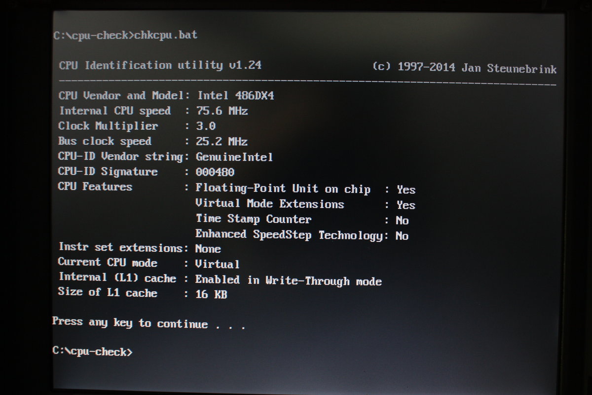
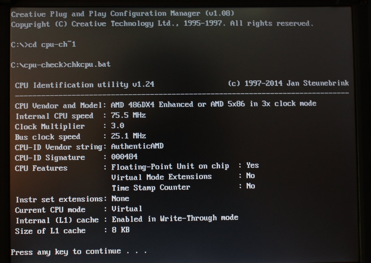
Here the CPU info I got from the standard Intel DX4 mainboard configuration using CHKCPU v1.24 (a simple but great tool):
The decoding table for the AVASEM chip gave the following frequency settings:
-
For the TP 701 standard bus: FS0=0 FS1=1 FS2=0 FS3=1 -> 25.06 MHz
-
This gives the desired AMx586-frequency: FS0=0 FS1=0 FS2=1 FS3=1 -> 33.29 MHz
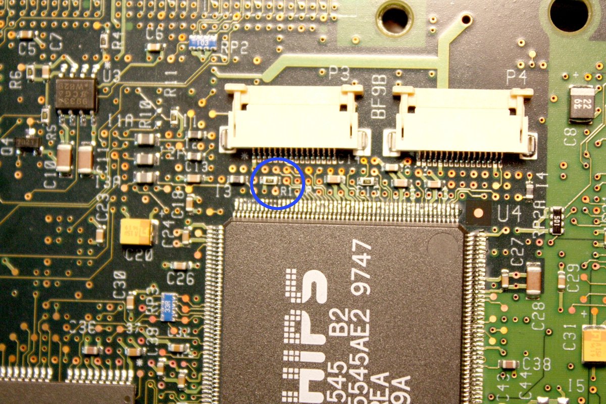
Here the corresponding Frequency Select Pins (FSPs) on the board:
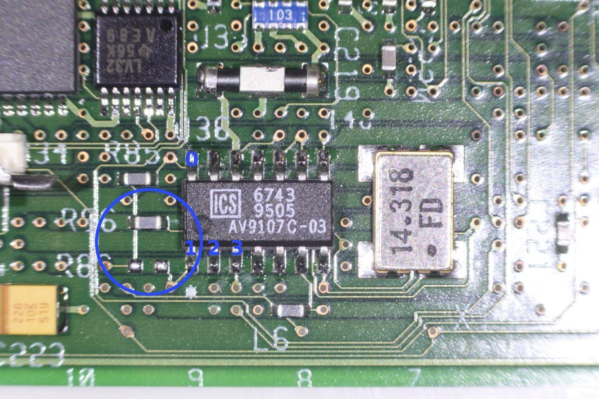
Notice something? The two grey smd resistors on the chip´s left set the corresponding FSP to "low" / zero. To get from 0101 in the photo to 0011, I simply had to put the second resistor one position lower (edit info: I had written capacitors here before which is indeed wrong - the credits go to zaprodk on hackaday for correcting me, thank you =-):
And a short test:

Okay - it worked - 100.4 Mhz. The overclocked DX4 works but gives "incorrect opcode" errors from time to time. As the original DX4 is not even intended to work on this frequency, I decided to continue with the AMx586.
AMD AMx586 CPU upgrade
The X5 is a low-power chip which uses a core voltage of 3.3 volts instead of the 5 volts used by 80486 desktop CPUs. Luckily the original DX4 is also powered by 3.3 volts and the pinout is more or less identical. This makes it unlikely that the 5x86 will get fried when used on the board.
I started with a standard non-overclocked DX4 board:

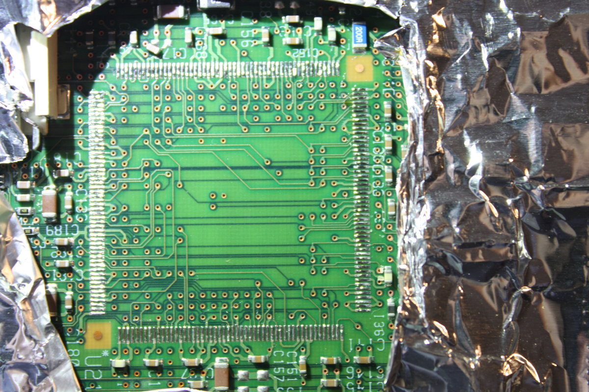
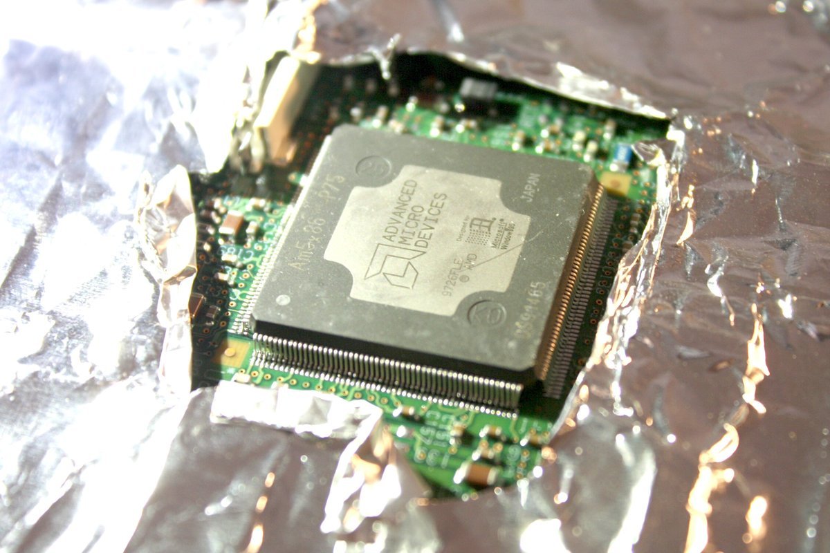
To prevent damages from excessive heat during the removal of the old chip, I wrapped the board with aluminum foil. With a stream of hot air I heated the chip up until the solder became fluid. Then I could lift the DX4 carefully up and put it away.

Afterwards, I cleaned the solder points on the board and put a fine amount of new solder to them.
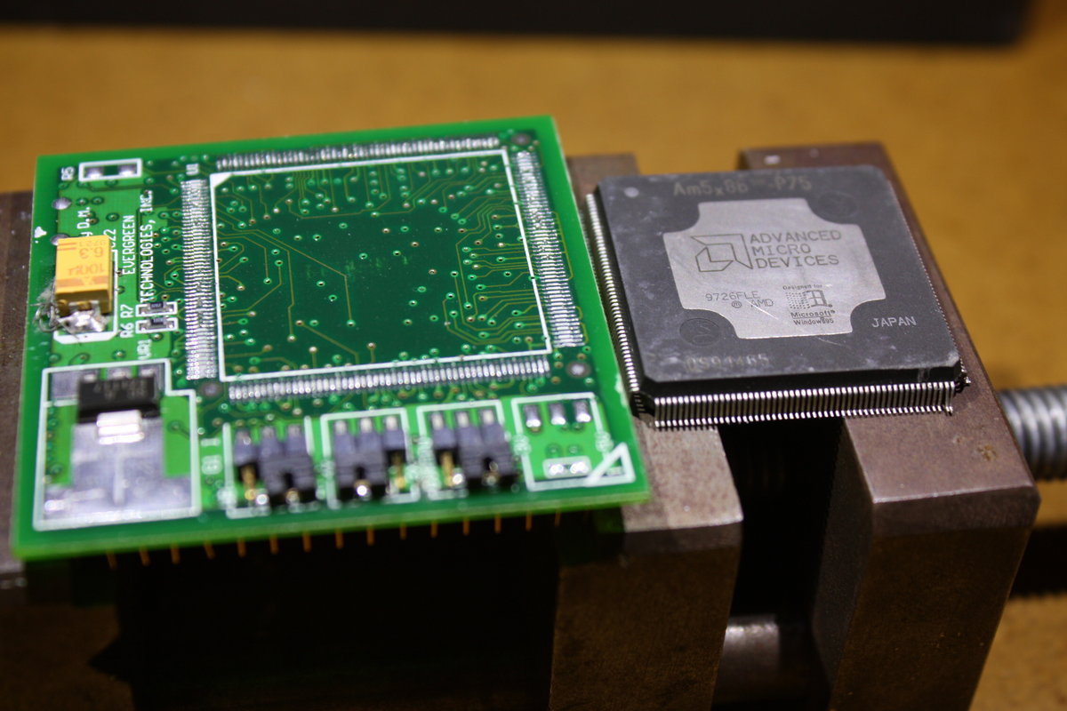
Now I checked my two X5 CPUs:
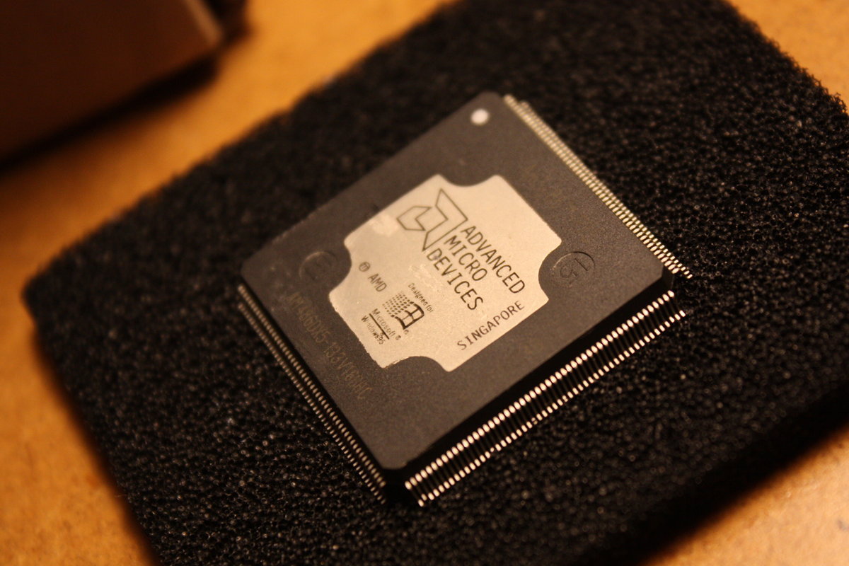
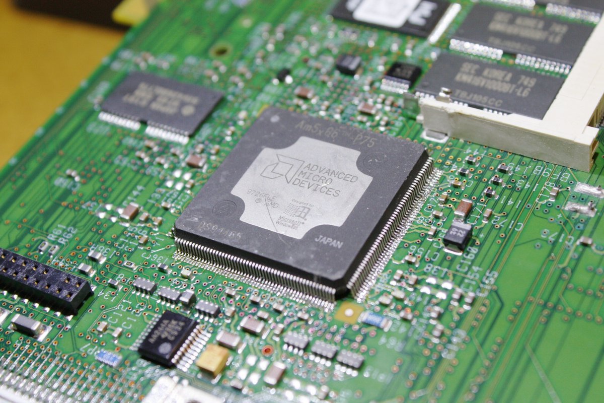
The first one was an unused AM486DX5-133V16BHC made for embedded x86-based applications.
The second one was soldered to an Evergreen 168-pin module.
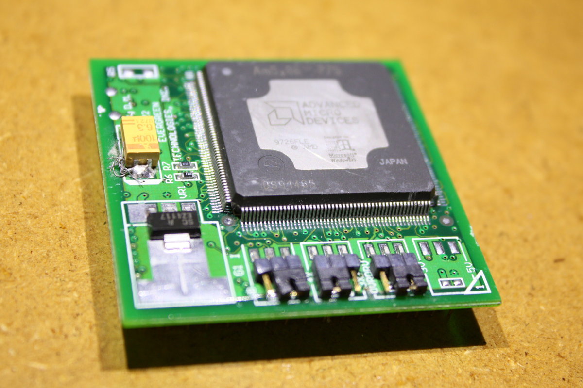
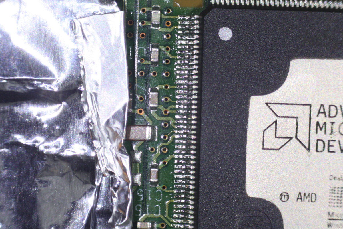
I removed the latter with hot air (for those interested the circuit traces under the butterfly DX4 and under the Evergreen X5):
Now I could align it on the butterfly board.
With a fine tip on my soldering iron I resoldered the pins and checked the solder joints under the microscope (this photo was taken from the AM486DX5-133V16BHC which I soldered to another board).
And finally, I had a successfully swapped CPU (here the AM486DX5-133V16BHC):
This is what the CPU identifier gave me now (the "Vendor string" has changed significantly =-):
I still had to raise the multiplier and bus clock speed. As for the latter I did it like described above.
Setting the correct clock multiplier
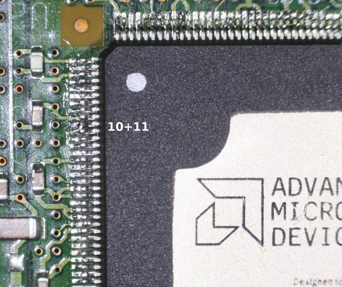
Again alldatasheet.com helped me on by providing a datasheet for the Am5x86 microprocessor. The tag "CLKMUL" gave me an important hint: "For 133-MHz processors, [CLKMUL] must always be connected to VSS [i.e. has to to be grounded] to ensure correct operation." - that means bridge CPU-pins 10 and 11 to get a 4.0-multiplier (I later verified this by inspecting the pins on the Evergreen module and it showed that the 4x mode was activated with a jumper which did just the same).
And another check:

Great, everything worked out as exspected. As the X5 has an internal 16K write-back cache, next step will be to get it activated.
Activating the internal write-back cache
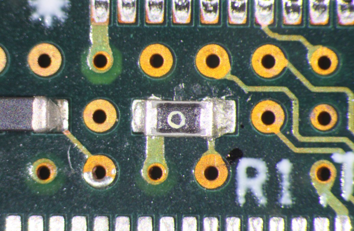
Again, the datasheet for the Am5x86 microprocessor delivered the answer: "If the processor samples [pin 64 tagged "WB/WT"] High at RESET, the processor is configured in Write-back mode". To get it "High", I looked for the easiest way to connect pin 64 to a Vcc pin. I determined pin 62 to be the closest one and interestingly R1 - a 100k resistor located on the other side of the mainboard - already connected pin 64 to pin 62.

I thus replaced the 100k with a zero-ohm-resistor as seen on the following picture.
This final modification gave me a permanently activated write-back cache - and a Am5x85-powered Thinkpad butterfly...

greetings noq2
Update
I´m looking for a working top system board to get my second Thinkpad butterfly (a Thinkpad 701CS) repaired. It already died many years ago after the faulty hibernation battery leaked =-(
If you can sell me one for a small amount of money, please post a comment below to get into contact with me - I would really appreciate it =-)
Comments